36
Connecting up the BPU
Last week I finished designing the final part of the BPU. Now it's time to connect everything together. It will not be as easy as it sounds, as there are still some small problems to resolve.
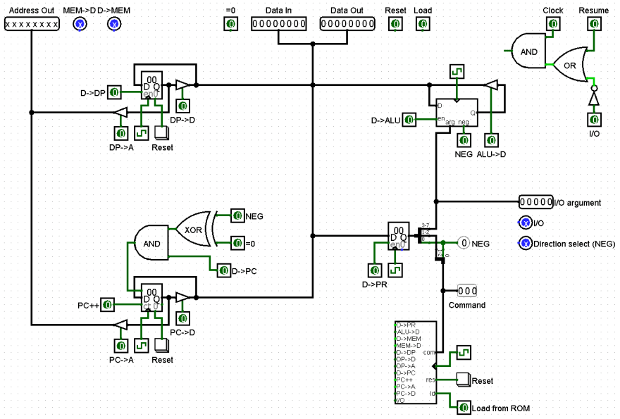
This is the arrangement of parts of the BPU in Logisim I designed a long time ago. You could see it in the github repo inside the Logisim file. Connecting up the BPU is initially straightdorward, as it starts with putting all the parts in their places and connecting them to the data lines.
Next step consists of adding all the other inputs and outputs needed for operation: control signals that go outside the BPU (
MEM->D, D->MEM, I/O, NEG), clock, reset, load from ROM, =0 input signal and the I/O argument line.Before connecting all the signals, there is an issue with the clock input that needs resolving. The BPU should be able to stop itself in order to wait for input/output and the I/O devices should be able to resume the BPU. The simplest way to stop operations is to stop the clock after it's falling edge, and that's what I will use in the BPU.
The clock should be tied low if the
The clock should be tied low if the
I/O signal is on, unless a new external Resume signal is on. This creates the following boolean function:Clock AND (Resume OR NOT I/O)Which can be added to the Logisim design.
If you think this image looks a bit crowded then brace yourself, because now it's finally time to connect all signals. If you're trying to replicate my work by yourself, make sure everything you've done up to this point is debugged to perfection and back your project up. No matter how hard you try, the BPU will look like a twisted mess of wires after this step. If you get the signals messed up it's sometimes easier to get back to the backup and rewire everything again. You have been warned.
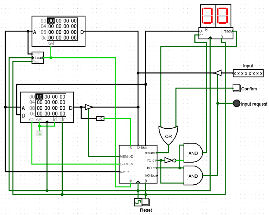
This is the general layout of the brainfuck computer in Logisim. The Data Bus is split in two parts due to the fact that Logisim can't handle input and output on the same pin, but they are connected inside the BPU so they should both carry the same data. The 5-bit I/O bus would be used if there were more I/O devices or if they were more complex, but it won't be used in this case.
After inserting the parts I noticed right away that some signals don't match: I/O devices have their respective enable signals, but the BPU only has general I/O enable signal and I/O direction select. Fortunately they are easy to convert from one to the other: input enable is on when I/O enable is on and the direction is 0, and output enable is on when I/O enable is on and the direction is 1. Another minor issue is having two
Resume signals feed into one input on the BPU, but that's easily fixed with an OR gate.Now all the parts are ready to be connected. Again, it's extremely important to have each and every part troroughly debugged and the project backed up because after connecting the signals debugging gets much harder.
And there you have it, ladies and gentlemen, a finished and working brainfuck computer. Now it's time to program this beauty and maybe add some more advanced I/O devices. Base Logisim offers a LED matrix, a TTY terminal and a keyboard interface, which is not far from a basic old-fashioned computer. Nevertheless this is the end of the base BPU series. Thanks for reading and hopefully see you again in future posts!
36


